Search This Blog

Wednesday, 2 July 2025

Cloud Computing Model as per NIST Definition

0 comments
  • In Cloud Computing model, the computing resources - be it a server hardware, storage, network, or application software - are available from the cloud vendor or provider's site/premises

  • Resources available on the cloud can be accessed over the Internet from any remote location and by any local computing device. 
  • In addition, the usage or accessibility is to cost only to the level of usage to the customers based on their needs and demands, also known as the pay-as-you-go or pay-as-per-use model.

Cloud Computing is a Service:
  • All the resources available on the cloud are considered as services that can be availed on demand.  
  • One such service available on the cloud is the storage service.  With the help of this service, we can store our family photographs, our favorite songs, and even movies on the cloud.
  • Flickr is an example for storage service on the cloud through which we can store our images and photos, as well as share them with others
  • Some of the advantages of using Flickr for storing our photos online are as follows:
    • Flickr allows us to easily access our images no matter where we are or what type of device we are using
    • Flickr lets us share the images
    • Flickr provides backup for our files. By uploading the images to Flickr, we are creating  backup on the web

Cloud Computing is a Platform:
  • The basic meaning of the term platform is that it is the base or ground that provides the support for applications to exist and run on a hardware. 
  • For example, Microsoft Windows is a platform on which application software can be installed and run for the user to interact.
  • The term platform refers not only operating system, but also many more in computer science:
    • Java is a platform even though it is not an operating system.  It provides the environment on which developers can develop and run applications of various kind using Java.
    • Similarly, the World Wide Web (WWW) can be considered as the operating system (or platform) for all our Internet-based applications.
  • In cloud computing model, WWW is a platform on which software such as Office 2.0, which was originally available on desktop computers, is now  available on the web.
  • Word processors like Buzzword and office suites like Google Docs are now available in the cloud as their desktop counter-parts.

Essential Characteristics of Cloud Computing:
  • As per the definition of NIST, cloud model is composed of five essential characteristics, three service models, and four deployment models.
  • Here is the description of those essential characteristics of Cloud Computing:
1. On-demand self-service: Consumers have the ability to independently and automatically provision computing resources—such as server time and network storage—without the need for direct human intervention with the service provider.  
  • This capability exemplifies the on-demand nature and elasticity of cloud services.
  • Examples of resources available on the cloud include storage, processing, memory, and network bandwidth.

2. Broad network access: Cloud resources are accessible via network connections using standard protocols and interfaces, which facilitate their use across diverse client devices, including mobile phones, laptops, and PDAs. 
  • This approach ensures broad compatibility and interoperability among heterogeneous platforms, supporting varied client environments

3. Elastic resource pooling: The provider’s computing resources are pooled to serve multiple consumers using a multitenant model, with different physical and virtual resources dynamically assigned and reassigned according to consumer demand.
  • There is a sense of location independence in accessing the cloud
  • The customer generally has no control or knowledge over the exact location of the provided resources but may be able to specify the location at a higher level of abstraction (e.g., country, state, or data center).

4. Rapid elasticity: Capabilities can be rapidly and elastically provisioned, in some cases automatically, to quickly scale out and rapidly released to quickly scale in.

  • To the consumer, the capabilities available for provisioning often appear to be unlimited and can be purchased in any quantity at any time.

5. Measured service: Cloud systems automatically control and optimize resource use by leveraging a metering capability at some level of abstraction appropriate to the type of service (e.g., storage, processing, bandwidth, and active user accounts).
  • Resource usage can be monitored, controlled, and reported providing transparency for both the provider and consumer of the utilized service.
Continue reading →
Monday, 30 June 2025

Introduction to Artificial Intelligence

0 comments
Artificial intelligence, or AI, refers to the simulation of human intelligence processes by computer systems.  It involves using algorithms and data to enable machines to perform tasks that typically require human intelligence, such as learning, reasoning, problem solving, and decision making.  AI can range from simple automation to complex deep learning and neural networks.

The internet has revolutionized connectivity and given us faster access to more information.  Distributed computing scales data processing, enabling efficiency.  IoT proliferates connected devices, generating massive amounts of data.  Social networking has encouraged most of us that data to be unstructured.  Together, they reshape our digital landscape, accelerating information access and innovation.

Human beings have innate intelligence, which is defined as the intelligence that governs every activity in our body.  The only innate intelligence machines have is what we give them.  We provide machines with the ability to examine examples and create machine learning models based on the inputs and desired outputs.  We do this in different ways, such as with supervised learning, unsupervised learning, and reinforcement learning.

Three Categories of Artificial Intelligence:

AI can be divided into categories based on strength, breadth, and application. 

Considering the strength of AI, it can be of three types - weak AI or narrow AI, strong AI or generalized AI, and super AI or conscious AI.  Weak or narrow AI is AI that is applied to a specific domain.  Applied AI can perform specific tasks but not learn new ones, making decisions based on programmed algorithms and training data.  For example, language translators, virtual assistants, AI-powered web searches, recommendation engines, and intelligent spam filters.

Strong AI or generalized AI refers to artificial intelligence capable of engaging in and performing a diverse array of distinct and unrelated tasks.  It possesses the ability to acquire new skills to tackle novel challenges, achieving this by autonomously learning fresh approaches.  Generalized AI is the combination of many AI strategies that learn from experience and can perform at a human level of intelligence.  Its use cases include finance, human resources, information technology, research and development, and supply chain.

Super AI or conscious AI extends the concept of generative AI to a more advanced level.  It is an AI with human-level consciousness, which would require it to be self-aware, showing advanced cognitive abilities and developing its own thinking skills.  Super AI could demonstrate capabilities beyond human intelligence in areas like healthcare, autonomous vehicles, robotics, natural language understanding, and environmental conservation.

Knowledge Required for Implementing AI:

Computer science and electrical engineering determine how AI is implemented in software and hardware.  Mathematics and statistics determine viable models and measure performance.

Because AI is modeled on how we believe the brain works, psychology and linguistics play an essential role in understanding how AI might work.  Philosophy, on the other hand, provides guidance on intelligence and ethical considerations.

Augmented Intelligence:

Artificial intelligence is the ability of a  machine to perform tasks that normally require human intelligence, such as reasoning, natural communication, and problem solving.  It basically replaces the need for a human.  So computers are doing the work, without the need for human intervention.  

Augmented intelligence is more than that of Artificial Intelligence.  It involves both man and the machine working together.  They're doing so to enhance each other's efforts when completing tasks.  Augmented intelligence systems augment our human abilities.  With the advent of AI, experts are encouraged to scale their capabilities and let the machines handle the time-consuming work.

Things like screen readers for the blind, voice-driven navigation, or driving a car having collision avoidance system, they're all examples of augmented intelligence at work.  They act on our behalf in the physical world, but in a way that complements our own capabilities.

Continue reading →
Saturday, 28 June 2025

Arithmetic Micro Operations

0 comments
  • Arithmetic micro operations are arithmetic operations such as Addition and Subtraction that are performed on the value of a register.
  • The simplest form of arithmetic micro operations are increment and decrement.  
  • Increment is nothing but adding value 1 to the existing content of the register.  Similarly decrement will reduce the existing value of a register by 1.
  • These micro operations are imple­mented with a combinational circuit or with a binary up-down counter.


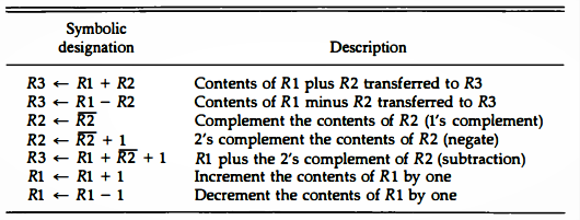
  • The symbolic representation of some of the micro operations are shown in the above table along with the description
  • Here is an arithmetic micro operation, which is represented using the Register Transfer Language (RTL) as follows:
                        R3 ← R1 + R2
  • It specifies the add micro operation, that adds the contents of register R1 with the contents of register R2, and the sum be transferred to register R3.
  • The arithmetic operations of multiply and divide are not listed in above Table. 
  • These two operations are valid arithmetic operations but are not included in the basic set of micro operations.
  • In most com­puters, the multiplication operation is implemented with a sequence of add and shift microoperations. 
  • Division is implemented with a sequence of subtract and shift micro operations.

Implementing Micro Operation - Add:
  • To implement the add microoperation with hardware, we need the registers that hold the data and the digital component that performs the arithmetic addition. 
  • The digital circuit that forms the arithmetic sum of two bits and a
    previous carry is called a full-adder
  • The digital circuit that generates the arithmetic sum of two binary numbers of any length is called a binary adder. 


4-bit Binary Adder

  • The binary adder is constructed with full-adder circuits connected in cascade, with the output carry from one full-adder connected to the input carry of the next full-adder.
  • The augend bits of A and the addend bits of B are designated by subscript numbers from right to left, with subscript 0 denoting the low-order bit. 
  • The carries are connected in a chain through the full-adders. 
  • The input carry to the binary adder is C0 and the output carry is C4 
  • The S outputs of the full-adders generate the required sum bits.

An n-bit Binary Adder:
  • An n-bit binary adder requires n full-adders. 
  • The output carry from each full-adder is connected to the input carry of the next-high-order full-adder.
  • The n data bits for the A inputs come from one register (such as R1), and the n data
    bits for the B inputs come from another register (such as R2).
  • The sum can be transferred to a third register or to one of the source registers (R 1 or R2), replacing its previous content.

Implementing Micro Operation - Subtract:
  • The Subtraction micro-operation can be done most conveniently by means
    of complements, i.e., taking the 2's complement of addend bits and adding it to the augend bits
  • For example, the subtraction A - B can be done by taking the 2's complement of B and adding it to A.
  • The 2's complement can be obtained by taking the 1' s complement and adding one to the least significant pair of bits. 
  • The 1's complement can be implemented with inverters and a one can be added to the sum through the input carry.
  • This adder-subtractor (subtraction through addition) operation can be combined into one com­mon circuit by including an exclusive-OR gate with each full-adder

4-bit adder-subtractor:
  • A 4-bit adder-subtractor circuit is shown in below figure. 
  • The mode input M controls the operation. When M = 0 the circuit is an adder and when M = 1 the circuit becomes a subtractor
  • Each exclusive-OR gate receives input M and one of the inputs of B. 

  • When M = 0, we have B  0 = B. The full-adders receive the value of B, the input carry is O, and the circuit performs A plus B 
  • When M = 1, we have B  1 = B' and C0 = 1. The B inputs are all complemented and a 1 is added through the input carry. 
  • The circuit performs the operation A plus the 2's complement of B
Binary Incrementer:
  • The increment microoperation adds one to a number in a register.
  • For example, if a 4-bit register has a binary value 0110, it will go to 0111 after it is incremented.
  • Every time the count enable is active, the clock pulse transition increments the content of the register by one.
  • The diagram of a 4-bit combinational circuit incrementer is shown in Fig. 4-8. 
  • One of the inputs to the least significant half-adder (HA) is connected to logic-1 and the other input is connected to the least significant bit of the number to be incremented.
  • The output carry from one half-adder is connected to one of the inputs of the next-higher-order half-adder.
  • The circuit receives the four bits from A0 through A3 adds one to it, and generates the incremented output in S0 through S3. 
  • The output carry C4 will be 1 only after incrementing binary 1111. This also causes outputs S0 through S1 to go to 0.
Continue reading →
Thursday, 26 June 2025

Bus and Memory Transfers

0 comments

  •  A typical digital computer has many registers, and paths must be provided to transfer information from one register to another. 
  • The number of wires will be excessive if separate lines are used between each register and all other registers i n the system. 
  • A more efficient scheme for transferring information between registers in a multiple-register configuration is a common bus system. 
  • A bus structure consists of a set of common lines, one for each bit of a register, through which binary information is transferred one at a time. 
  • Control signals determine which register is selected by the bus during each particular register transfer.

Use of Multiplexer in Bus Transfer:
  • One way of constructing a common bus system is with multiplexers. 
  • The multiplexers select the source register whose binary information is then placed on the bus. 
  • The construction of a bus system for four registers is shown in Fig. 4-3. 
  • Each register has four bits, numbered 0 through 3. 
  • The bus consists of four 4 x 1 multiplexers each having four data inputs, 0 through 3, and two selection inputs, S1 and S0
  • The bits in the same significant position from each register are connected to the data inputs of one multiplexer to form one line of the bus. 
  • Thus MUX 0 multiplexes the four 0 bits of the registers, MUX 1 multiplexes the four 1 bits of the registers, and similarly for the other two bits. 

Bus Selection for 4-bit Registers:
  • The two selection lines S1 and S0 are connected to the selection inputs of all four multiplexers. 
  • The selection lines choose the four bits of one register and transfer them into the four-line common bus. 
  • When S1S0 = 00, the 0 data inputs of all four multiplexers are selected and applied to the outputs that form the bus. This causes the bus lines to receive the content of register A since the outputs of this register are connected to the 0 data inputs of the multiplexers. 
  • Similarly, register B is selected if S1S0 = 01, and so on. 

  • Table 4-2 shows the register that is selected by the bus for each of the four possible binary value of the selection lines.
  • In general, a bus system will multiplex k registers of n bits each to produce an n-line common bus. 
  • The number of multiplexers needed to construct the bus is equal to n, the number of bits in each register. 
  • The size of each multiplexer must be k x 1 since it multiplexes k data lines.
8-bit Multiplexer for Data Transfer:
  • For example, a common bus for eight registers of 16 bits each requires 16 multiplexers, one for each line in the bus. 
  • Each multiplexer must have eight data input lines and three selection lines to multiplex one significant bit in the eight registers.
Symbolic Representation of Data Transfer in a Bus:
  • The transfer of information from a bus into one of many destination registers can be accomplished by connecting the bus lines to the inputs of all destination registers and activating the load control of the particular destination register selected. 
  • The symbolic statement for a bus transfer may mention the bus or its presence may be implied in the statement. 
  • When the bus is explicitly mentioned in the statement, the register transfer is represented as follows:
BUS ← C,
R 1 ← BUS
    • This symbolic representation implies that the content of register C is placed on the bus, and the content of the bus is loaded into register R 1 by activating its load control input. 
    • If the bus is known to exist (implicitly) in the system, it may be convenient just to show the direct transfer.
    R1 ← C

    Three-State Bus Buffers:
    • A bus system can be constructed with three-state gates instead of multiplexers. 
    • A three-state gate is a digital circuit that exhibits three states.
    • Two of the states are signals equivalent to logic 1 and 0 as in a conventional gate.  The third state is a high-impedance state.
    • The high-impedance state behaves like an open circuit, which means that the output is disconnected and does not have a logic significance.
    • Three-state gates may perform any conventional logic, such as AND or NAND.

    Memory Transfer

    • The transfer of information from a memory word to the outside environment is called a read operation.
    • A memory word will be symbolized by the letter M .
    • The particular memory word among the many available is selected by the memory address during the transfer.
    • It is necessary to specify the address of M when writing memory transfer operations.
    • This will be done by enclosing the address in square brackets following the letter M .
    Memory Read:
    • Consider a memory unit that receives the address from a register, called
      the address register, symbolized by AR .
    • The data are transferred to another register, called the data register, symbolized by DR.
    • The read operation can be stated as follows:
                    Read: DR ← M [AR]
    • This causes a transfer of information into DR from the memory word M selected by the address in AR.
    Memory Write:
    • The write operation transfers the content of a data register to a memory word M selected by the address.
    • Assume that the input data are in register Rl
    • R2' is the symbol for the 1's complement of R2.
    • Adding 1 to the 1' s complement produces the 2' s complement.
    • Adding the contents of R1 to the 2' s complement of R2 is equivalent to R1 - R2.
    • The result will be stored in R3 by transferring the data from ALU to R3 via the central bus and then to the external memory using its memory address. 

    Continue reading →
    Tuesday, 24 June 2025

    Transferring Data using Memory Data Register (MDR)

    0 comments

    Fetching and Storing Data using MDR

    • With few exceptions, an instruction can be executed by performing one or more of the following operations in some specified sequence:
      1. Fetch the contents of a given memory location and load them into a processor register
      2. Transfer a word of data from one processor register to another or to the ALU
      3. Perform an arithmetic or a logic operation and store the result in a processor register
      4. Store a word of data from a processor register into a given memory location

    Memory Read and Write Operations using MDR:
    • During memory Read and Write operations, the timing of internal processor operations must be coordinated with the response of the addressed device on the memory bus.
    • The processor completes one internal data transfer in one clock cycle. 
    • The speed of operation of the addressed device, on the other hand, varies with the device.
    • To accommodate the variability in response time, the processor waits until it receives an indication that the requested Read operation has been completed.
    • We will assume that a control signal called Memory-Function-Completed (MFC) is used for this purpose.
    • The addressed device set this signal to 1 to indicate that the contents of the specified location have been read and are available on the data lines of the memory bus.
    Fig.: Connection and Control Signals for MDR

    • The connections for register MDR are illustrated in the figure shown above. 
    • It has four controls signals: MDRin and MDRout control the connection to the internal bus, and MDRinE and MDRoutE control the connection to the external bus.

    Fetching a Word from Memory
    • To fetch a word of information from memory, the processor has to specify the address of the memory location where this information is stored and request a Read operation.
    • This applies whether the information is to be fetched represents an instruction in a program or an operand specified by an instruction.
    • The processor transfers the required address to the MAR, whose output is connected to the address lines of the memory bus. 
    • At the same time, the processor uses the control lines of the memory bus to indicate that a Read operation is needed. 
    • When the requested data are retrieved from the memory they are stored in register MDR, from where they can be transferred to other registers in the processor.

    Example for Reading Data from Memory:
    • As an example of a read operation, consider the instruction Move (R1), R2. The actions needed to execute this instruction are:
    1. MAR ← [R1]
    2. Start a Read operation on the memory bus
    3. Wait for the MFC response from the memory
    4. Load MDR from the memory bus
    5. R2 ← [MDR]
    • These actions may be carried out as separate steps, but some can be combined into a single step. 
    • Each action can be completed in one clock cycle, except action 3 which requires one or more clock cycles, depending on the speed of the addressed device.

    Register Transfer 
    • Instruction execution involves a sequence of steps which may involve data transfer from one register to another.  
    • For each register, two control signals are used in order to perform any one of the following operations:
      1. Place the contents of the register on the bus (Write) 
      2. Load the data on the bus into the register (Read)
    • The input and output of register Ri are connected to the bus via switches controlled by the signals RiIn and RiOut, respectively.
    • When RiIn is set to 1, the data on the bus are loaded into Ri. Similarly, when RiOut is set to 1, the contents of Register Ri are placed on the bus.
    • While Riout is equal to 0, the bus can be used for transferring data from other registers.
    • Suppose that we wish to transfer the contents of register R1 to register R4. This can be accomplished as follows:
      • Enable the output of register R1 by setting R1Out to 1. This places the contents of R1 on the processor bus.
      • Enable the input of register R4 by setting R4In to 1. This loads data from the processor bus into register R4.

    Storing a Word in Memory:
    • Writing a word into a memory location follows a similar procedure.
    • The desired address is loaded into MAR. Then, the data to be written are loaded into MDR, and a Write command is issued.
    • The executing of instruction Move R2, (R1) requires the following sequence:
      1. R1out , MARin
      2. R2out, MDRin, Write
      3. MDR out E, WMFC
    • As in the case of the read operation, the Write control signal causes the memory bus interface hardware to issue a Write command on the memory bus. 
    •  The processor remains in step 3 until the memory operation is completed and an MFC response is received
    Continue reading →
    Friday, 20 June 2025

    Role of a CPU in Program Execution

    0 comments

    Fundamental Concepts of Program Execution

    • A typical computing task consists of a series of steps specified by a sequence of machine instructions that constitute a program
    • To execute a program, the processor fetches one instruction at a time and performs the execution specified in that machine instruction
    • Instructions are fetched from successive memory locations until a branch or a jump instruction is encountered

    Organization of a Digital Computer
    • In addition to ALU, CPU consists of a Control Unit (CU) and a number of registers for storage and execution of machine instructions
    • The coordination among various units of a computer such as memory, ALU and input and output units are coordinated by the control circuitry (also called Control Unit)


    Here is a Presentation on the Role of a CPU.


    Program Counter (PC):
    • The processor keeps track of the address of the memory location containing the next machine instruction to be fetched using a special register called Program Counter (PC)
    • After fetching an instruction using PC, the contents of the PC will be updated to point to the next machine instruction available in the sequence
    • A branch instruction may load a different value (memory address) into the PC.

    Instruction Register (IR):
    • Another key register available in the processor is the Instruction Register (IR)
    • IR holds the instruction that is currently being executed in the CPU
    • The instruction available in IR is decoded by the CPU and the necessary signals are generated by the CU to control the various processing elements involved in executing the machine instruction being decoded 
    • Suppose that an instruction occupies 4 bytes in memory, it has to go through the following three-step process in the CPU for its execution:  
    Step-1: Fetch the contents of the memory location pointed to by the PC. The contents of this location are interpreted as an instruction to be executed. Hence, they are loaded into the IR. Symbolically, this an be written as 
                    IR  [[PC]] 
    Step-2: Assuming that the memory is byte addressable, increment the contents of the PC by 4, that is,
                                        PC [PC] + 4
    Step-3: Carry out the actions specified by the instruction in the IR.
    • In cases the instruction being executed occupies more than one word (4 bytes), steps 1 and 2 must be repeated as many times as necessary to fetch the complete instruction. 
    • The first two steps are usually referred to as the fetch phase: step 3 constitutes the execution phase.


    Internal Organization of the Processor:
    • A simple organization of a Processor is given below:

    • In this simple organization of a processor, the Arithmetic and Logic Unit (ALU) and all the registers are interconnected via single common bus. 
    • The bus is internal to the processor (called CPU Bus) and should not be confused with the external bus that connects the processor to the memory and I/O devices. 
    • The data and address lines of the external memory bus are (shown in the above figure) connected to the internal processor bus via the memory data register, MDR, and the Memory Address Register (MAR), respectively.

    MDR, MAR and IR:
    • Register MDR has two inputs and two outputs. Data may be loaded into MDR either from the memory bus or from the internal processor bus for input. 
    • The data stored in MDR may be placed on either bus for output. 
    • The input of MAR is connected to the internal bus, and its output is connected to the external bus. 
    • The output of the Instruction Register (IR) is connected to the instruction decoder and control logic block, which is responsible for issuing the signals that control the operation of all the units inside the processor and the external memory.

    Other Registers Inside the CPU:
    • The number and use of the processor registers R0 through R(n-1) vary considerably from one processor to another. They are provided for general-purpose use by the programmer. 
    • Some may be dedicated as special-purpose registers, such as index registers or stack pointers.  Three registers, X, Y, and TEMP are shown in the above figure.
    • Special-purpose registers are not meant for the programmer, that is, the programmer need not be concerned with them because they are never referenced explicitly by any instruction.
    • They are used by the processor for temporary storage during execution of some instruction.
    • These registers are never used for storing data generated by one instruction to be used by another instruction at a later stage.

    ALU and Control Unit (CU):
    • As instruction execution progresses, data are transferred from one register to another, often passing through the ALU to perform some arithmetic or logic operation. 
    • The instruction decoder and control logic unit is responsible for implementing the actions specified by the instruction loaded in the IR register. 
    • The decoder generates the control signals needed to select the registers involved and direct the transfer of data.
    • The registers, the ALU, and the interconnection bus are collectively referred to as the datapath.

    Performing Arithmetic or Logical Operation in ALU:
    • The ALU is a combinational circuit that has no internal storage. It performs arithmetic and logic operations on the two operands applied to its A and B inputs. 
    • As shown in the figure above for internal organization of a processor, one of the operands is the output of the register X and the other operand is obtained directly from the bus.
    • The result produced by the ALU is stored temporarily in register Y. 
    •  Therefore, a sequence of operations need to be performed to add the contents of register R1 to those of register R2 and store the result in register R3:
        1.  R1out , Xin 
        2.  R2out, Xout, Yin 
        3.  Yout, R3in
    • The signals whose names are given in any step are activated for the duration of the clock cycle corresponding to that step. All other signals are inactive. 
    • Hence, in step 1, the output of register R1 and the input of register X are enabled, causing the contents of R1 to be transferred over the bus to X.
    • In step 2, the output of register R2, and the output of register X are enabled, causing the content of R1 and R2 to be added by the ALU.

    Storing the Result in R3:
    • The function performed by the ALU depends on the signals applied to its control lines. 
    • In this case, the Add line is set to 1, causing the output of ALU to be the sum of the two numbers given as input A and B. 
    • The result of this addition is loaded into register Y because its input control signal is activated. 
    • In step 3, the content of register Y is transferred to the destination register, R3. 
    • This last transfer can' t be carried out during step 2, because only one register output can be connected to the bus during any clock cycle.

    Continue reading →
    Wednesday, 18 June 2025

    Register Transfer Language (RTL)

    0 comments

    Role of Registers and Register Transfer Language

    • A register is a group of flip-flops with each flip-flop capable of storing one bit of information. 
    • An n-bit register has a group of n flip-flops and is capable of storing any binary information of n bits. 
    • In addition to the flip-flops, a register may have combinational gates that perform certain data-processing tasks. 
    • In its broadest definition, a register consists of a group of flip-flops and gates that effect their transition. 
    • The flip-flops hold the binary information and the gates control when and how new information is transferred into the register. 

    Micro Operations on Registers in a CPU:
    • Digital modules are best defined by the registers (one of the digital component) they contain and the operations that are performed on the data stored in them.
    • Similarly, the internal operation of a digital computer is mainly determined by the following factors: 
      1. The set of registers (called general purpose registers) a CPU contains for internal storage of data to be processed
      2. The sequence of operations (called micro operations) performed on the binary information stored in the registers 
      3. The control that initiates the micro operations on the data available in registers
    • The operations executed on data stored in registers are called micro operations
    • micro operation is an elementary operation performed on the information stored in one or more registers. Examples of micro operations are shift , count, clear, and load. 
    • The result of a micro operation may replace the previous binary information of a register or transfer the content of one register to another register. 
      • For example, a counter with parallel load is capable of performing the micro-operations increment and load.
      • A bidirectional shift register is capable of performing the shift right and shift left micro operations.


    Register Transfer Language (RTL)
    • It is possible to specify the sequence of micro operations in a computer by explaining every operation in words, but this procedure usually involves a lengthy descriptive explanation. 
    • It is more convenient to adopt a suitable symbology to describe the sequence of transfers between registers and the various arithmetic and logic micro operations associated with the transfers. 
    • The use of symbols instead of a narrative explanation provides an organized and concise manner for listing the micro operation sequences in registers and the control functions that initiate them.
    • The symbolic notation used to describe the micro operation transfers among registers is called a Register Transfer Language (RTL) 


    • The term "register transfer" implies the availability of hardware logic circuits that can perform a stated micro operation and transfer the result of the operation to the same or another register. 
    • In general, a programming language is a procedure for writing symbols to specify a given computational process. 
    • A register transfer language is a system for expressing in symbolic form the micro operations that will take place using the registers of a digital module. 
    • It is a convenient tool for describing the internal organization of digital computers in concise and precise manner.

    Symbolic Representation of Registers in Micro Operations:
    • Computer registers are designated by capital letters (sometimes followed by numerals) to denote the function of the register. 
    • For example, the register that holds an address for the memory unit is usually called a Memory Address Register and is designated by the name MAR.
    • Other examples for registers are PC (for Program Counter), IR (for Instruction Register, and R1 (for processor register).
    • The most common way to represent a register is by a rectangular box with the name of the register inside, as in Fig. 4-1(a). 
    • The individual bits can be distinguished as in (b). 
    • The numbering of bits in a 16-bit register can be marked on top of the box as shown in (c). 

    Program Counter (PC):
    • A 16-bit register is partitioned into two parts in Fig. 4-1(d). Bits 0 through 7 are assigned the symbol L (for low byte) and bits 8 through 15 are assigned the symbol H (for high byte). 
    • Program Counter (PC) is an example of 16-bit register, which keeps track of the address of the next instruction to be fetched and executed. 
    • The symbol PC(0-7) or PC(L) refers to the low-order byte and PC(S-15) or PC ( H) to the high-order byte.

    Register Transfer:
    • Information transfer from one register to another is designated in symbolic form by means of a replacement operator (ß
    • The statement 
                    R2 ß R1 
             denotes a transfer of the content of register R1 into register R2. 
    • It designates a replacement of the content of R2 by the content of Rl. 
    • By definition, the content of the source register R1 does not change after the transfer. 
    • A statement that specifies a register transfer implies that circuits are available from the outputs of the source register to the inputs of the destination register and that the destination register has a parallel load capability.
    Basic Symbols for Register Transfer:
    • The basic symbols of the register transfer notation are listed in Table 4-1. 
    • Registers are denoted by capital letters, and numerals may follow the letters.
    • Parentheses are used to denote a part of a register by specifying the range of bits or by giving a symbol name to a portion of a register.
    • The arrow denotes a transfer of information and the direction of transfer. 
    • A comma is used to separate two or more operations that are executed at the same time.
    • The statement 
                        T: R2 ß R1, R1 ß R2 
              denotes an operation that exchanges the contents of two registers during one common clock pulse provided that T = 1. 
    • This simultaneous operation is possible with registers that have edge-triggered flip-flops.
    Continue reading →